We use KiCad to design schematics and printed circuit boards. We use KiCad version 9.0. This page does not describe the design process for making PCBs. To get introduced to KiCad we recommend you see the following resources:
Making a New Project
Opening KiCad for the first time will show the project manager. When making a new project you can set the name and location. Ensure create a new folder for the project is clicked. Your project will come with .kicad_pro, .kicad_sch, and .kicad_pcb files. These extensions correspond to the project, schematic and PCB files.
Terminology
- Footprint: the physical layout of copper pads, holes, and outlines of a specific electronic component
- Symbol: a standardized simple graphic that represents an electronic components
- PCB Layout: the physical representation of the schematic with footprints positioned
Schematics
In KiCad you start projects by making a schematic. Most of the basics of the schematic editor in KiCad is standard across all guides. One of the most difficult part of making a schematic in KiCad is finding the right symbols, and linking the symbols to the correct footprint.
KiCad comes with a large symbol library but it may not have the symbol you need. If you need extra symbols you can make your own in the symbol editor or find it online. Symbols can be found online from a distributor, manufacturer, or user maintained repositories. Most of the time extra symbols can be found online. The same is true for footprints, KiCad has a large library but often you will have to find footprints online. We recommend the following resources to find extra resources:
- Digikey Electronic components distributor
- SnapMagic PCB footprints and schematic symbols
- Octopart Electronic part search engine
It is important to organize the symbols and footprints you download in the project folder so that other people can edit your project. It ultimately does not matter the exact way you structure the folders but it is important that it is consistent. To find an example project folder structure see Recommended Project Structure. You may not know the exact components or footprints you will use until you start making your PCB.
You may run out of space in your schematic. To get around this, use hierarchical schematics. Hierarchical schematics are like windows to extra pages that you can link to with labels or flags.
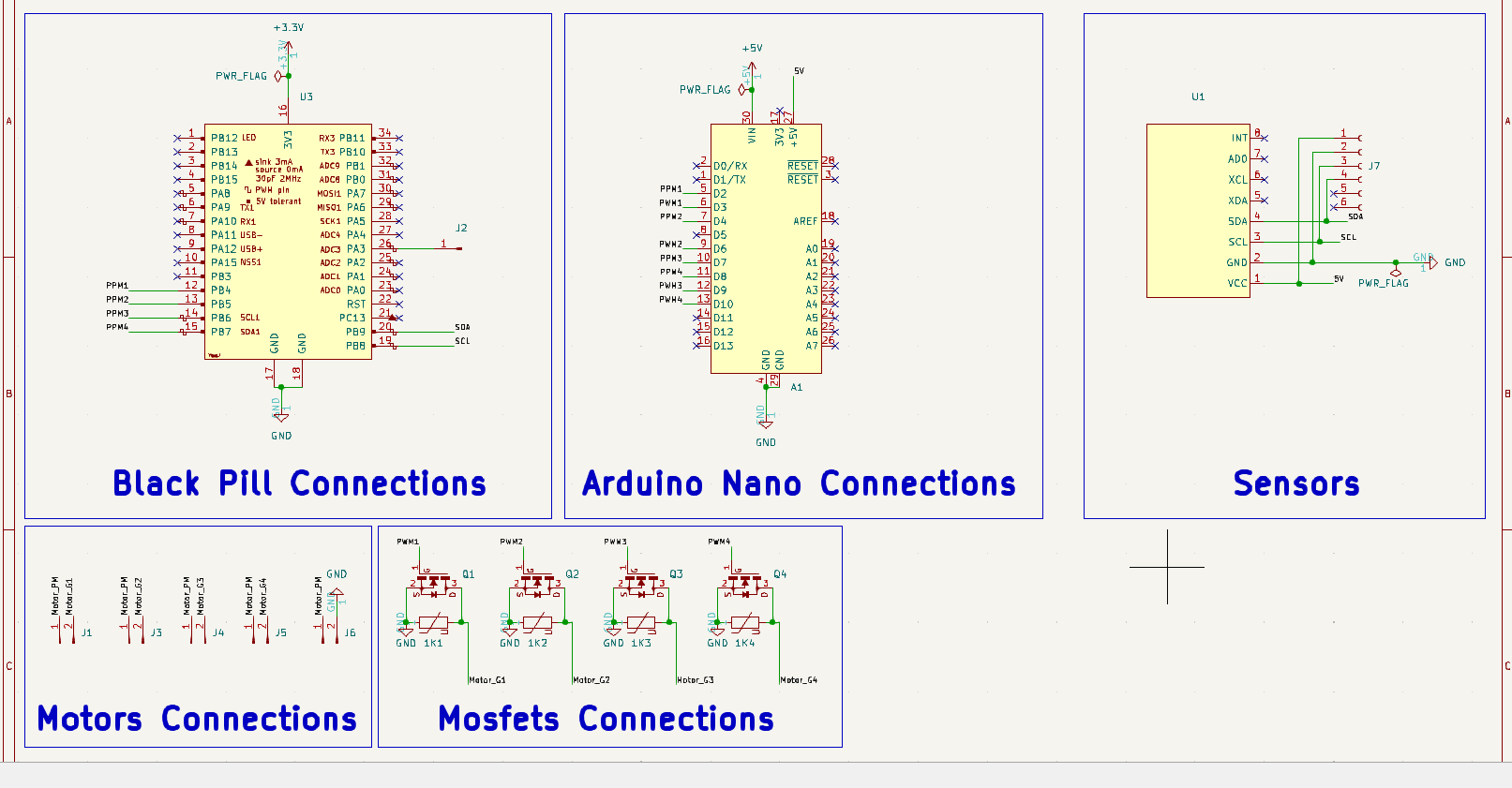
Before you move on from the schematic phase, run an Electrical Rules Check to verfiy that you are not breaking any basic rules and check that you linked all of your symbols to footprints. Press the Assign Footprints... button to link symbols to footprints. Additionally, try to organize the schematic into sections that correspond to functions within the circuit and add labels/titles to the sections. An example of a clean schematic can be seen below.
PCB Layouts
After a schematic is created you can begin to lay out your PCB. By default KiCad has the PCB configured as a 2 layer board which is suitable for most of our boards. Before you begin your layout set some default sizes for traces. A good rule of thumb is 0.2 to 0.3mm for signals and 1mm for power traces up to 2 Amps. KiCad will add all of the footprints you linked in the schematic phase to the PCB layout window when you press the Update PCB from Schematic... button. ALl of the footprints will appear in a clump with blue lines between pads if everything has been setup properly so far. These blue lines show the connections that need to be made with traces.
Recommended Project Structure
This example uses neptune as the project name. The root folder should be named the same as the project name. Use dashes to separate words in the project name. In this example triton is a component that has a footprint .kicad_mod, a symbol .kicad_sym, a 3D model .step, and a Datasheet .pdf. Organize files for a component in a folder that is placed in a dependencies folder, this way when another person opens up the project KiCad will know where to find the files.
neptune/
├── dependencies
|   └── triton
|       ├── triton.kicad_mod
|       └── triton.kicad_sym
|       └── triton.step
|       └── triton.pdf
├── neptune.kicad_pcb
├── neptune.kicad_sch
├── neptune.kicad_pro
└── README.md